Today, on my way to work, I walked past the Heinrich Hertz lecture hall on the KIT campus – the place where he originally discovered electromagnetic waves between 1895 and 1899. His portrait is displayed on the historic center of the KIT campus, and you barely even notice it if you don’t know of its existence. In our research project we simulate the propagation of exactly these waves in Photonic Wire Bonds. Here is why we do this:
Do you know Moore’s law? What it states is pretty simple and not as much a law as an observation:
Every two years, the number of transistors doubles.
Transistors are the elemental building-block for any logical system and crucial for the amount of computations (and complexity thereof) a chip can handle. So the continuous increase of the number of transistors on a chip correlates with the amount of information it can process (input-data) and the amount of results it can generate (output-data). Modern computers however do not consist of one single chip doing all the work – they consist of thousands of specialized chips that rely on many others to function. This creates a need for fast communication between chips and here “fast” means:
On the one hand you want low latency – meaning a signal should take a short time to get from one chip to the next. On the other hand you want high bandwidth – meaning a lot of data should be transported in a short window of time.
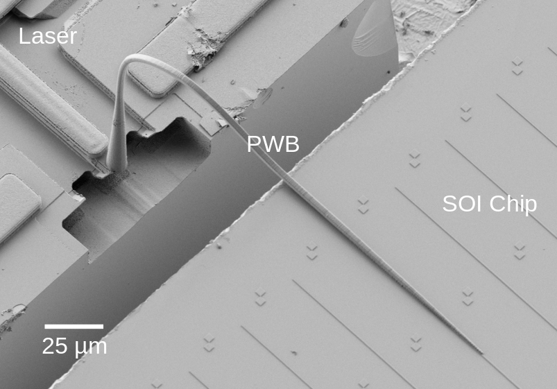
Illustration 1: A Photonic Wire Bond (PWB) connecting two chips. See also: M. R. Billah, et al. “Multi-Chip Integration of Lasers and Silicon Photonics by Photonic Wire Bonding”
Conf. on Lasers and Electro-Optics (CLEO’15), San Jose (CA), USA, May 10–15 , paper STu2F.2. Optical Society of America (OSA) (2015)
For all these reasons our work is focused on the design of Photonic Wire Bonds (PWB) – photonic chip-to-chip interconnects. You can imagine that these wire bonds work just like water pipes: An ideal water pipe transports water without spilling or spoiling any of it. In our case the pipe is a freeform polymer structure and the water is light. Unfortunately, bent wire bonds always leak out light. Since the width of the wire bond is similar to the wavelength of the light propagating in it, we can see and simulate the wave-like properties of light in this setting.
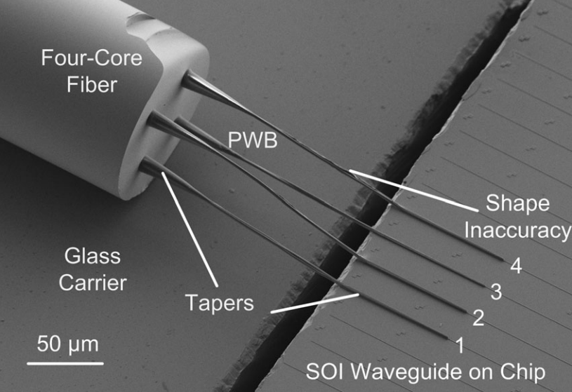
Illustration 2: A Multicore Fibre connected to a Silicon Photonic Circuit. See also: N. Lindenmann, et al. “Connecting Silicon Photonic Circuits to Multicore Fibers by Photonic Wire Bonding” J. Lightwave Technol. 33, 755-760 (2015)
In the project C4 we focus on the shape optimization of wire bonds to reduce radiation losses and negative effects on the quality of the signal. We aim at laying the mathematical groundwork for low latency – high bandwidth optical chip-to-chip interconnects as seen in illustration 1. If all goes well we hope to also be able to take a look at more intriguing shapes such as those shown in figure 2 and 3. As a reference: a human hair usually has a diameter of 100 μm!
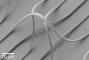
Four Photonic Wire Bonds on a flat surface. See also: C. Koos, et al. “Three-dimensional two-photon lithography: an enabling technology for photonic wire bonding and multi-chip integration”
Proc. SPIE 8970 (LASE-SPIE’14), Laser 3D Manufacturing, March , 897008-897008-10 (2014) (invited)
Tonight, when I leave the office to go home, I will walk by the Institute of Photonics and Quantum Electronics – the place where Prof. Dr. Christian Koos and his research group produce such structures for testing. The illustrations 1-3 as well as the underlying concepts and physical laws controlling electromagnetic waves were created and discovered just a few hundred meters from my office. Can you imagine any better location to do mathematical research on wire bonds?